Workflow
LiNPhA specializes in designing, fabricating and characterizing electro-optic thin-film lithium niobate devices. Our workflow looks as follows:
Simulation and design
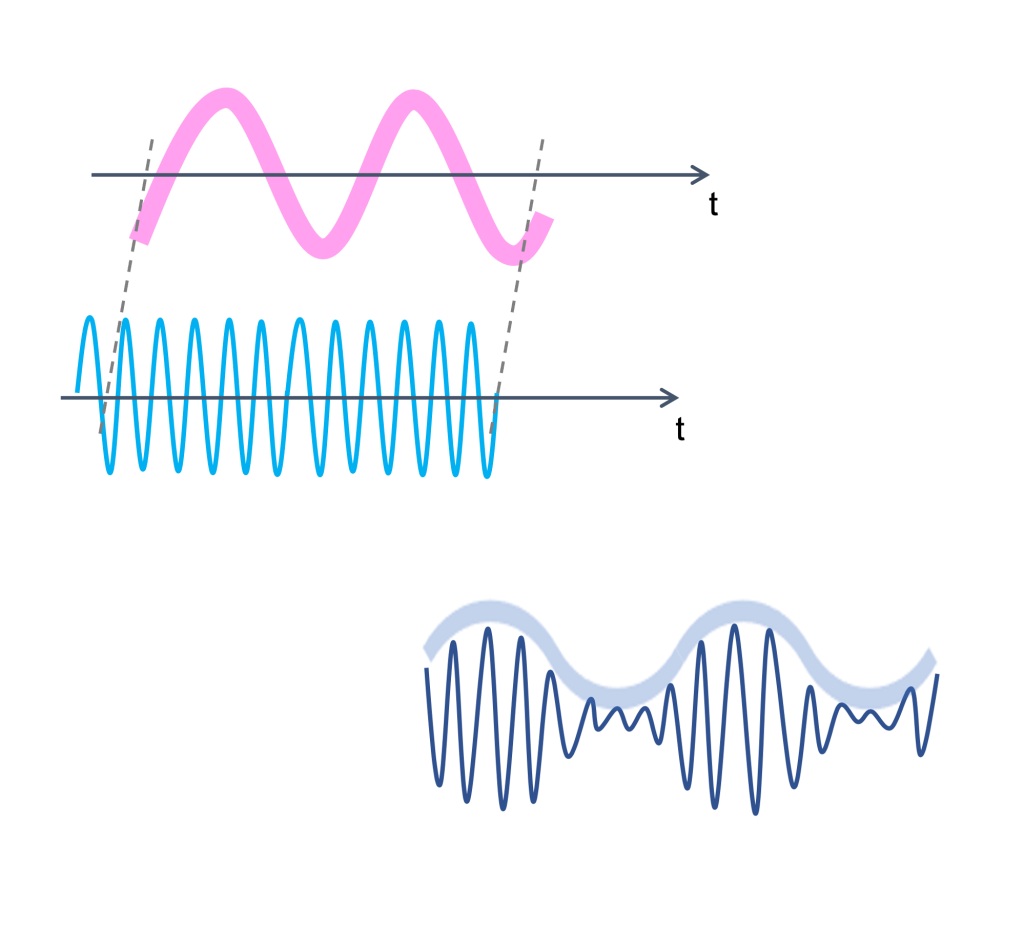
To provide effective modulators it is essential to co-design the photonic and the electrical part of our devices. This ensures that the optical and the RF signals travel at the same speed (so-called velocity matching), leading to optimal electro-optic response.
Fabrication of optical circuit
We specialize in micro- and nano-structuring commercially available thin-film lithium niobate wafers obtaining diverse photonic components on a chip using an LN-dedicated fabrication processes.


Fabrication of RF circuit
The RF electrodes, permitting to interface the optical signal travelling in the LN waveguide with an electrical signal, are fabricated with standard microfabrication processes. DC electrodes are also implemented in this step.
Validation
Finally the devices are validated using optical and electronic test facilities. The response is compared to the expected (simulated) performance.

Below is an overview of thin-film lithium niobate as a photonic platform.
Thin-Film Lithium Niobate
Lithium Niobate (LN) is a crystal with numerous properties interesting for a broad range of applications. At LiNPhA we concentrate on its photonic applications: due to its peculiar crystal structure, this material is ideal to implement electro-optic devices (meaning components whose optical properties can be tuned using an external “electrical knob“) and efficient non-linear optical devices (that are components permitting to change the frequency of the light travelling through them). Thanks to these features, LN crystals have been for decades a crucial building block for a wide range of optical systems.
The main drawback of “old-style” LN devices is their large footprint and limited scalability. However between 2010 and 2020 great efforts have been put into producing sub-micron-thick layers of LN which, mimicking the geometry of silicon on insulator (SOI), hold promise for highly scalable and mass producible lithium niobate on insulator (LNOI) devices.
Nowadays such thin-film lithium niobate (TFLN) wafers are commercially available and small footprint TFLN photonic integrated circuits (PICs) can be implemented. The reduction in footprint allows:
- High scalability of the fabrication process.
- Improved electro-optical performance
(3x Bandwidth, up to -90% Power consumption).
TFLN phototnic integrated circuits can compete both in terms of scalability and footprint with other PICs platforms (such as InP and SOI), with the advantage of highly efficient linear electro-optic properties which other materials cannot provide and that make TFLN PICs the number one candidate for high performance optical modulators.
LN is an inert material, meaning that traditional cleanroom processes (developed for III-V semiconductors and Silicon-based devices) are not effective to micro- and nano-structure the thin-film LN.
To date, there is not a standardized, high volume foundry service for this material. LiNPhA’s team has over 7 years of cleanroom experience, most of which spent in developing and optimizing fabrication processes for LN optical devices. The image below shows an overview of the fabrication process of the optical circuit.

If you have any curiosity about the possibility that this platform offers or want to know more about our expertise, contact us at info@linpha.se.